
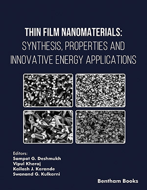
Abstract
Several scholars and scientists have recently continued their efforts to fabricate and
develop advanced nanomaterials in the form of nanoparticles, clusters, emulsions, and thin
films to design nanoscopic optoelectronic devices, supercapacitors, solar systems, and
biomedical equipment. Because of the widespread exceptional physiochemical characteristics
and improved functionalities, hybrid nanostructures, including organic and inorganic metaloxides, sulphides and polymeric nanostructures are highly appreciated and explored for
enhanced physicochemical, biological, and environmental applications. Therefore, metalsulphides nanomaterials such as CdS, ZnS, MoS2, and PbS, as nano-thin films were widely
designed, and employed in various geometries such as 1D, 2D, and 3D nano-thin films, which
possess extraordinary functionality. Among them, MoS2 (molybdenum disulfide) is considered
as an emerging class of semiconducting material due to its direct bandgap value i.e. (~1.9 eV),
has high current on/off ratio (108
) at normal temperature, and exhibited mobility 200 cm2 Vs−1
.
It has the ability to change its architecture from bulk to nanoscale level. On the basis of its
unique structure, MoS2 has two characteristics: (i) it possesses a hexagonal structure with SMo-S layers arrangement by covalent bond, and (ii) Van der Waals force of interaction that lies
between the adjacent layers of MoS2, which makes it suitable for multiple applications.
Moreover, the structural, surface, and optical properties of MoS2 are altered by the
stoichiometric doping of metal/ions, which favour its electronic features toward improved work
functionalities. This chapter will provide a systematic explanation for the synthesis, design,
morphological investigations, and developments of the MoS2 semiconducting nano-thin films
for multiple optoelectronic, biochemical, and environmental uses.
Keywords: 2D nano-thin films, MoS2, Modified structures and surfaces, Solar cells, Sensor applications.
Related Journals

Related Books
Advanced Materials and Nano Systems: Theory and Experiment - Part 2

Advanced Materials and Nano Systems: Theory and Experiment (Part-1)

The Art of Nanomaterials

Nano Materials Induced Removal of Textile Dyes from Waste Water
Nanobiotechnology: Principles and Applications
Bio-Inspired Nanotechnology
Synthesis of Nanomaterials
Materials Science: A Field of Diverse Industrial Applications
Synthesis and Applications of Semiconductor Nanostructures

Industrial Applications of Polymer Composites