
Abstract
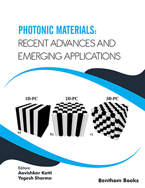
As the world is modernizing, it is noteworthy to mention photonics and its categorization based on size. Despite the components of light being invisible to the human eye, nature never ceases to amaze us with its idiosyncratic phenomenon. Furthermore, the manipulation of the matter is confined to the nanoscale as a part of the progression. Adding nanotechnology to photonics emerges out as nanophotonics which is the cutting-edge tech of the twenty-first century. Human beings have acclimated to the concept of photonics, furthermore, nanophotonics is the science of miniaturization study, potentially helping the technology to modify itself into the sophistication of the equipment and thereby be of assistance in various disciplines of science and technology. One can illustrate nanophotonics by considering the fabrication processes of nanomaterials. In variegated applications, these nanoscale processes will refine and produce structures with high precision and accuracy. Meanwhile, groundbreaking inventions and discoveries have been going around, from communications to data processing, from detecting diseases to treating diseases at the outset. As one stresses on the idea of nanophotonics, it never reaches a dead-end, however, this explains how vast the universe and each of the components co-existing are infinitesimally beyond humans' reach. Nevertheless, nanophotonics and its applications bring about remarkable multidisciplinary challenges which require proficient and well-cultivated researchers. Despite the fact it has several advantages, it carries its downside, which requires a detailed analysis of any matter. Using state-of-the-art technology, one can constrict light into a nanometer scale using different principle methodologies such as surface plasmons, metal optics, near field optics, and metamaterials. The distinctive optical properties of nanophotonics call out specific applications in the electronics field such as interaction chips, tiny devices, transistor filaments, etc. When compared to conventional electronic integrated circuits, the pace at which data using nanophotonic devices is sent is exceptionally fast, accurate, and has a better signal processing capability. As a result of the integration of nanotechnology with photonic circuit technology, high-speed data processing with an average processing speed on the order of terabits per second is possible. Furthermore, nano-integrated photonics technology is capable of comprehensive data storage and processing, which inevitably lays the groundwork for the fabrication, quantification, control, and functional requirements of novel optical science and technology. The maj-ority of applications include nanolithography, near-field scanning optical microscopy, nanotube nanomotors, and others. This explains about the working principle, different materials utilized, and several other applications for a better understanding.
Keywords: Metal Optics, Near Field Optics, Metamaterials, NEMS, Surface Plasmons.
Related Journals

Current Physics
Related Books

Practical Handbook of Thermal Fluid Science

Digital Signal Processing in Experimental Research

Frontiers in Nuclear and Particle Physics

Frontiers in Nuclear and Particle Physics

Advances in Classical Field Theory

Open Quantum Physics and Environmental Heat Conversion into Usable Energy

Open Quantum Physics and Environmental Heat Conversion into Usable Energy

Open Quantum Physics and Environmental Heat Conversion into Usable Energy
Progress in Computational Physics (PiCP)

Progress in Computational Physics (PiCP)